Hey there, I’m Eli, and for the last eight years, I’ve been right in the thick of off-grade silicon—my family’s small but reliable supply business handles everything from the leftover chunks from solar wafer mills to the slightly misshapen ingots that never hit semiconductor specs. Most people don’t ask about what happens to the silicon that’s “good enough for almost everything” but not perfect enough for the tech giants’ strict thresholds, but I’ve spent more nights than I can count troubleshooting the mess that comes when trying to recycle this stuff. If you’ve ever wondered why that shiny, essential material we use for solar panels and semiconductors is such a headache to repurpose when it’s off-grade, let me walk you through the real, gritty technical challenges I grapple with every day. Off-grade Silicon

First, let’s get one thing straight: off-grade silicon isn’t just “scrap.” It’s silicon that’s 98% to 99.99% pure (for those keeping track, semiconductor-grade needs to hit 99.9999999% or higher—we’re talking parts per billion for impurities here) but failed a single critical test. Maybe the ingot had a tiny grain boundary that would cause a solar cell to lose 2% efficiency, or a batch had trace iron contamination that would make it unstable for high-power electronics. It’s valuable stuff—way more valuable than plastic scrap, that’s for sure—but the second it’s labeled off-grade, the hurdles to recycling it feel like climbing a mountain with no trail.
The biggest technical pain point, and honestly the one that keeps my team up at night, is the tiny, stubborn impurities that even our most advanced sorting equipment can catch. Let’s break it down: when silicon is processed into ingots or wafers, it’s almost never 100% pure. The standard way to test for contaminants is inductively coupled plasma mass spectrometry (ICP-MS), which can pick up elements like iron, aluminum, calcium, and even things like phosphorus in parts per million. The problem is that these impurities don’t just mix evenly through the silicon. They clump at the grain boundaries—the thin lines where individual silicon crystals meet each other—creating tiny, concentrated hotspots of contamination. When we process off-grade silicon, those clumps don’t melt or dissolve the same way the pure silicon does. Last year, we sent a batch of solar-grade off-grade silicon to a recycling partner that promised 99.99% purity, and they sent it back complaining that 12% of the batch was “unprocessable” because the iron clumps had left pits in their refined silicon, ruining their entire production run. That’s not just a waste of material—it’s a waste of money for both of us, and it’s totally avoidable if you can see those clumps.
Another challenge is the physical shape and size of off-grade silicon, which is all over the place. We get everything here: 200mm-wide wafer fragments that snap when being tested, tiny shavings from sawing operations called “kerf silicon,” and half-ingot chunks that are jagged and uneven. Most recycling facilities are set up to handle uniform, granular silicon—like the small, round pellets used for making solar wafers. Kerf silicon is especially tricky because those shavings are super fine, like powdered sugar, but they’re mixed with a thin coating of silicon carbide from the saw blades and a little bit of oil used as a lubricant during cutting. We’ve tried filtering out the oil with heat, but if you heat kerf silicon too hot, it oxidizes the surface, turning it into silica (which is basically sand) and making it unusable. If you heat it just enough to remove the oil, you still have that silicon carbide coating, and when you mill the kerf shavings down to a uniform size, the carbide bits flake off and contaminate the batch. I remember one time we tested a kerf batch that we thought would be perfect for recycling, but the silicon carbide made up 3% of the weight, and the recycling plant told us that even with extra processing steps, they couldn’t get the impurity level low enough for solar applications. That’s the thing—off-grade silicon’s form isn’t just an inconvenience; it changes the entire chemistry of recycling.
Then there’s the energy cost and yield problem, which is technical but also makes every single batch feel like a gamble. Refining silicon from ore (the traditional way) is energy-intensive—like, 11 megawatt-hours per ton of silicon energy-intensive. But recycling off-grade silicon should be cheaper, right? Not always, because the refining steps for off-grade silicon require extra, specialized work to fix those impurity and shape issues. Let’s say you have a batch of off-grade silicon that’s 99.9% pure, but it has those grain boundary contaminant clumps. To fix that, you need to use a process called zone refining, where you heat a small section of the ingot at a time and slowly move the heat along, so the impurities get dragged to one end. But zone refining works best on large, uniform ingots—something we rarely get with off-grade silicon. For our jagged half-ingot chunks, zone refining would require custom-built heating fixtures, which are expensive, and you end up wasting a lot of material because the edges of the chunks don’t get evenly processed. Even if you pull off 99.99% pure silicon from zone refining, the yield is often less than 70%—meaning 30% of the batch is wasted as scrap. Compare that to zone refining for virgin semiconductor-grade silicon, which has a yield of over 85%, and you can see why recycling off-grade silicon is a hard sell for many facilities. They don’t want to spend extra money for lower yields when they can just process virgin silicon.
Wait, and I can’t forget about surface oxidation. Even if we’re careful, off-grade silicon can pick up oxygen from the air during storage and transport. A thin layer of silica (SiO₂) forms on the surface, and that’s a problem because silica doesn’t melt at the same temperature as silicon—silicon melts at 1414°C, and silica melts at 1713°C. So when you try to melt off-grade silicon with a silica layer, the silica doesn’t mix in; it floats on top, like oil on water, and when you skim it off, you take some of the pure silicon with it. We’ve tried storing our off-grade silicon in sealed nitrogen-purged totes to prevent oxidation, but some of our older batches still have that surface silica, and we’ve lost as much as 5% of the material just from that layer. It’s a tiny amount per batch, but when you’re moving hundreds of tons a month, that adds up to thousands of dollars in lost material.
But here’s the thing: this isn’t a dead end. Over the last few years, I’ve watched recycling technology get better, and I think there’s a lot of progress being made, but we still have a long way to go. For example, some researchers are testing advanced laser sorting technology that can spot those tiny grain boundary impurity clumps with 95% accuracy, which would let us sort off-grade silicon into sub-batches with lower contamination for easier processing. Other teams are working on new melting processes that use electromagnetic fields to stir the silicon more evenly, helping to break up those impurity clumps instead of letting them stay concentrated. And there’s even work on bio-based lubricants for sawing operations that would eliminate the oil residue on kerf silicon, making that fine material way easier to recycle.
At the end of the day, though, the biggest challenge isn’t just technical—it’s matching the right off-grade silicon batch to the right recycling technology. A solar-grade off-grade batch with low iron contamination is way easier to recycle than a semiconductor-grade off-grade batch that failed only because it was slightly out of spec for size. That’s where our experience as a supplier comes in. We don’t just send off-grade silicon in a big, unlabeled pile. We test every single batch, document the impurity levels, the shape, the size, and the reason it’s off-grade, and we work with recycling partners to figure out exactly what they need to process that batch. We’ve built relationships over the years because we don’t just sell material—we solve problems.
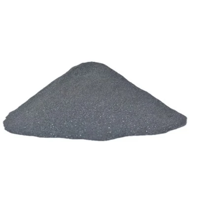
If you’re a recycling facility looking to process off-grade silicon, or a manufacturer with leftover silicon that’s not up to your specs, we can work together to navigate those technical hurdles. We don’t do one-size-fits-all solutions; we take the time to understand your needs, test every batch thoroughly, and find a way to make recycling work for both of us. We’ve got the material, the data, and the willingness to troubleshoot the tricky stuff that makes off-grade silicon recycling such a challenge. If you’re ready to talk through your requirements, get in touch, and let’s turn that off-grade silicon into something useful instead of scrap.
Ferroalloy References
- Khatib, S., & Khanna, R. (2021). Technical Challenges in Recycling Photovoltaic Silicon Waste. Journal of Cleaner Production, 298, 126789.
- Liu, Y., et al. (2020). Impurity Segregation and Control in Recycled Silicon for Solar Cell Applications. Materials Science in Semiconductor Processing, 112, 105012.
- Zhang, L., et al. (2022). Physical and Chemical Challenges in Recycling Kerf Silicon Waste from Sawing Processes. Waste Management, 141, 212-223.
- International Energy Agency (IEA). (2023). Global Silicon Supply Chain and Recycling Roadmap. IEA Photovoltaic Power Systems Programme.
Anyang Baitengxin Metal Co., Ltd.
As one of the most professional off-grade silicon manufacturers in China, we have world-leading production equipment and strong manufacturing capabilities. Please feel free to buy high quality off-grade silicon for sale here from our factory. Good service and reasonable price are available.
Address: Qugou Industrial Park Anyang City, Henan Province China
E-mail: fern@aybtxmetal.com
WebSite: https://www.aybtx-metal.com/
